This is the first part of a blog about putting a wifi router into a phone charger. Join us on Discord here. Check out the Github.
WiFi Pineapples are well-known tools in the security community. For those unfamiliar, Pineapples are purpose-built routers to be used in network attacks and exploits. With a Pineapple, you can perform man-in-the-middle attacks, network deauthing and password sniffing. Gilfoyle and Elliot used them in popular shows such as Mr. Robot and Silicon Valley. Hak5 had made a splash in the security community when they created the Pineapple, but I think there’s one major flaw: The form factor.
The Pineapple is a router, and, well, it looks like a router. However, there is no reasonable situation where an IT person would be cool with you plugging a router into their network. This is why I’m putting a WiFi router into a 5V wall adapter.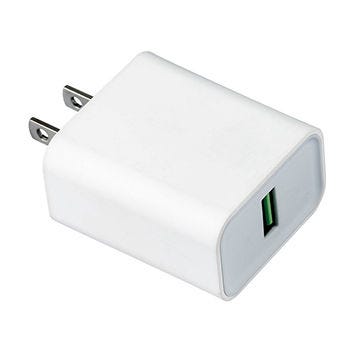
Drop one of these in a Mcdonald’s, and nobody’s going to expect a thing. You can leave it for days, while it collects data and marshals it back to your home network.
As for the methodology, I’m using 100% open-source CAD software. KiCad will be used to design the boards and FreeCad for all the mechanical work. BuildRoot or openWRT will be compiling the OS, and I’m booting an open-source OS on my home machine. The design is 100% open-source, schematics, board layout, gerbers and mechanical. All licenced under MIT.
That covers the concept; let’s get into the design. This design requires a microprocessor (MPU) with decent mainline Linux support, USB, MMU, SDIO and a clock rate north of 1Ghz. An MPU has a memory management unit (MMU), while a microcontroller (MCU) does not. An MMU is a special piece of IP that maps virtual memory (The relative memory address application are using) to physical memory (the actual address in the RAM or disk). An MMU is mandatory for Linux, and we need Linux for its network stack.
I ended up choosing the Allwinner A33; it’s an older MPU that came out in 2014. Tablet manufacturers used it in their Android devices, and since Android uses Linux, we should get good mainline support. It’s a quad-core 1.2Ghz processor with all the expected peripherals: USB, I2C, SPI, SDIO, RTC and PWM. It’s a nice little processor, and you can pick them up for < 10$. For non-volatile storage, I chose to use an SD card. For RAM, I’m going with an AS4C512M16D3L-12BIN, a 1GB low-power DDR3 IC. One nice thing about DDR3 is all the chips are pin/pin, so if you want to reduce your BOM, you can use a chip with less memory.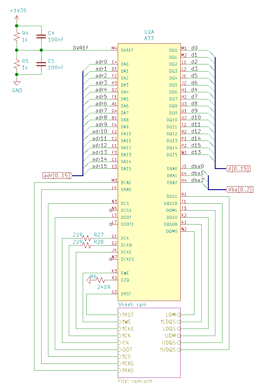
Pictured above is the connection from the DDR3 RAM controller on the A33 MPU to the RAM sheet; that little purple box is the sheet, not the part. I hope it’s pretty obvious what’s going on; the chip support two ranks; however, I’m using the one. Schematic capture for RAM is pretty straightforward; the routing is when it gets exciting.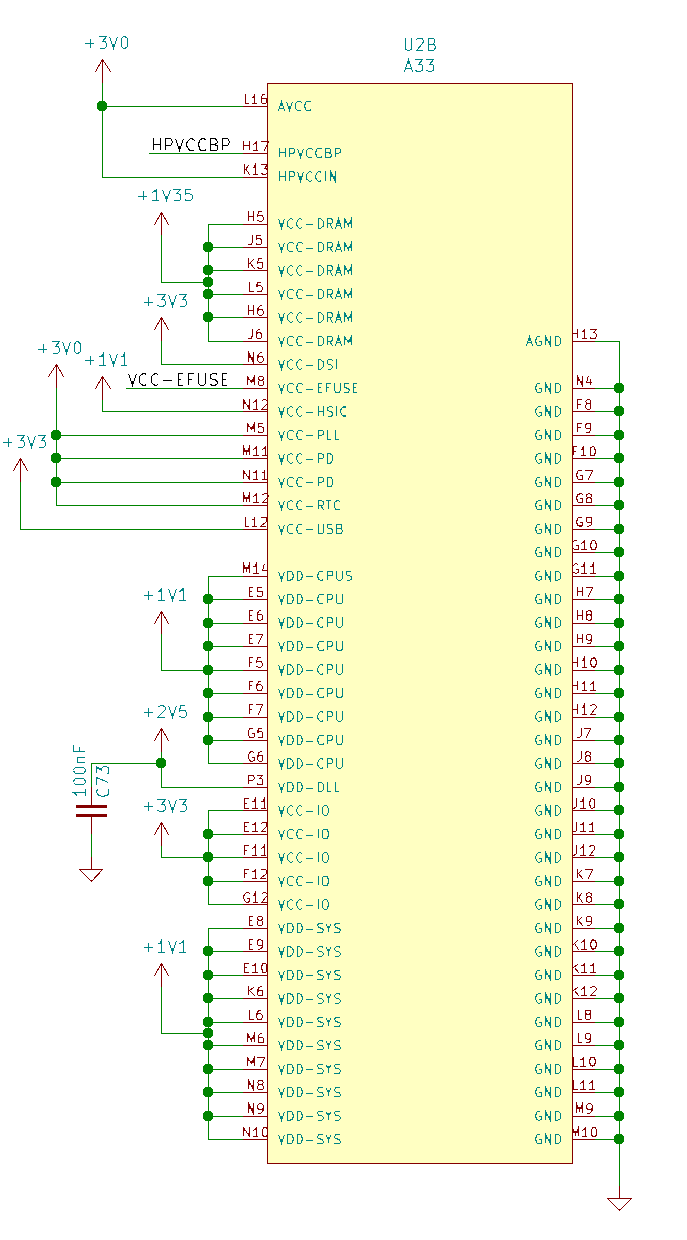
Powering an MCU is simple: typically, 3.3V is regulated down internally. That luxury goes out the window when you start working with the big boys; this chip needs five different voltage rails.
- Ram is 1.35V
- Cores are 1.1V
- DLL needs 2.5V (delay-locked loop btw)
- Analogs need 3.0V
- IO needs 3.3V
Oh, and there’s a sequence the rails need to come up at…
Every rail except the 2.5V requires a peak load of around 2A, so it’s time to pick out some switch mode power supplies! I liked the look of the TPS62095RGTR, and the datasheet says it has decent efficiency, which is important for thermals. I picked a CoilCraft XAL4020 inductor as they usually have the lowest DC resistance. This supply has a soft start pin which I can use to sequence the rails.
I will ignore the “powered from mains” requirement for this round of the board and feed in 5V elsewhere. Once the boards arrive, I need to analyze the allowable ripple into the supplies to size the capacitor on the output of the full-wave rectification bridge.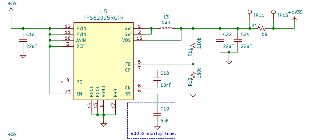
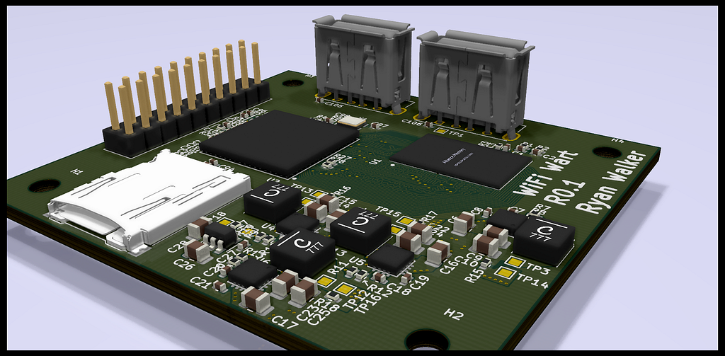
To wire in the radios, I’m currently placing USB-A jacks which will plug into two wifi dongles. This will work until I can settle on a part; currently, I quite like the RTL8188CUS. The nice thing about this module is you can buy the USB version of it online for cheap, so moving to the solder-down module isn’t much work.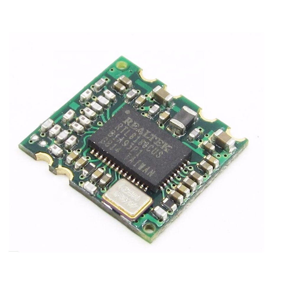
The non-volatile memory (NVM) for the device is an SD card; this connects over an SDIO interface and isn’t very interesting. Here’s a picture for completeness.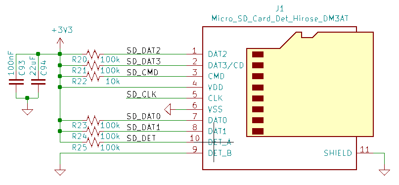
Once all of this is connected up, we _should _have a fully booting computer, assuming we have the correct image flashed to the SD card.
The next installment of this blog will feature more of the board layout; I want to talk about routing DDR3, power supplies and BGA packages! Until then, I’ll leave you with a render of the unfinished board!