This project is effectively “building a computer from scratch”; RAM, disk, USB and a processor. Our computer will be running a full-fledged operating system capable of installing programs, managing a network stack, playing games and even browsing the internet. However, we’re not going to be playing any games. This post is going to outline board layout, BOM generation, assembly and PCB bring up.
Board Layout
The schematic is the logical connection of the components, while the layout is the physical connection. So the first task is to set up the design rules in KiCad. I’m planning on using JLCPCB’s four-layer service; their capabilities can be found here. Rather than putting the exact capabilities in, I typically round the numbers up; you don’t want to be designing on edge.
DDR3 RAM
I chose the AS4C512M16D3L-12BIN, a 1GB DDR3L SDRAM IC housed in a 96 pin BGA package.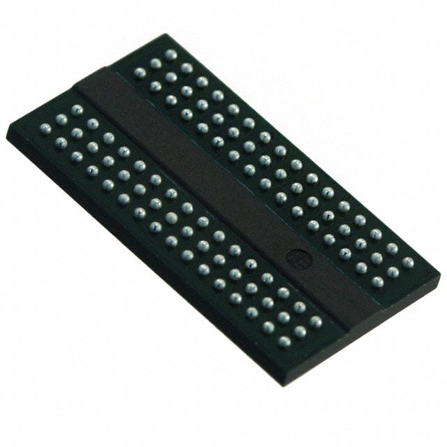
There are many things to consider when routing DDR3, firstly, the part placement. You may be tempted to place it as close to the processor as possible, and even if this is ideal for signal integrity (SI), it may make routing impossible. The A33-OLinuXino gerbers outline nice placement.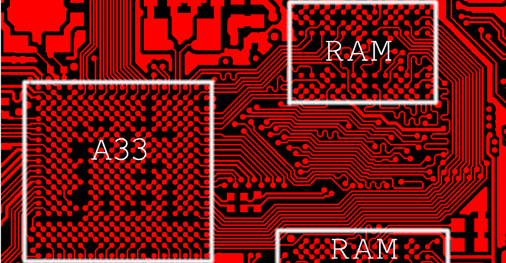
Olimex also went for a four-layer board, and the top and bottom layers were almost purely signalling. The designer used the two inner layers for GND and power distribution. They used two RAM ICs as the A33 supports two ranks. The upper and lower data bytes were routed to the upper and lower RAM chips, respectively. This makes routing nice, as byte groups don’t have to be length matched to each other, just length matched within their group.
I placed my RAM to the top right of the A33, and this would allow me to drop in some vias and pull down the signals pretty easily if I ever needed another RAM IC. Below are the length matching requirements I used.
CK/!CK: 0.2mm
addr[0:15], !WE, !CS, !RST, DBA[0:2], ODT, !CKE, CAS, RAS: 3mm
DQ[0:7]: 1.27mm
DQ[8:15]: 1.27mm
To further elaborate on these numbers, CK/!CK should be within 0.2mm of each other, DQ[0:7] should be within 1.27mm of each other, etc. These numbers came from a document and experience doing this type of work.
Kicad is getting good; it ships with a nice length tuning tool. To start, I found the longest trace, which turned out to my 40mm; I then set the target to 40mm. After that, you click other traces to match, and it will automatically add the little squiggles to lengthen the trace. My one gripe is KiCad doesn’t add the via length to the total track length. To account for this, I just ensured matched traces have the same numbers of vias.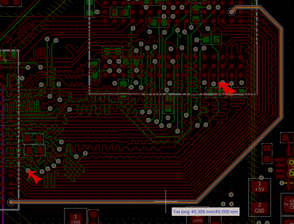
Power Supplies
As outlined in the last post, I chose the TPS62095RGTR to power the rails with higher current requirements. This switch-mode power supply (SMPS) operates in the buck (step down) configuration. I went with switching power supplies over linear power supplies for their efficiency improvement. It’s pretty simple to calculate the max efficiency of a linear power supply - it is denoted by the equation below.
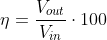
For example, if I used an LDO for my 1.1V supply derived from 5V, we’re looking at an absolute max efficiency of 22%. Where does the remaining power go? Heat! Since I’m building a small enclosed thing, I don’t want 5 watts of heat melting the enclosure. To get higher efficiency, you need switching supplies. They’re more efficient as (loosely speaking) they convert DC to AC and then back to DC using magnetics.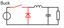
That switch is a transistor that is PWMing the input voltage. The LC filter then converts the PWM signal back into DC, which is consumed by the load.
So you have to be very considerate when laying out a supply like this; the first aspect to consider is the supply’s hot loop.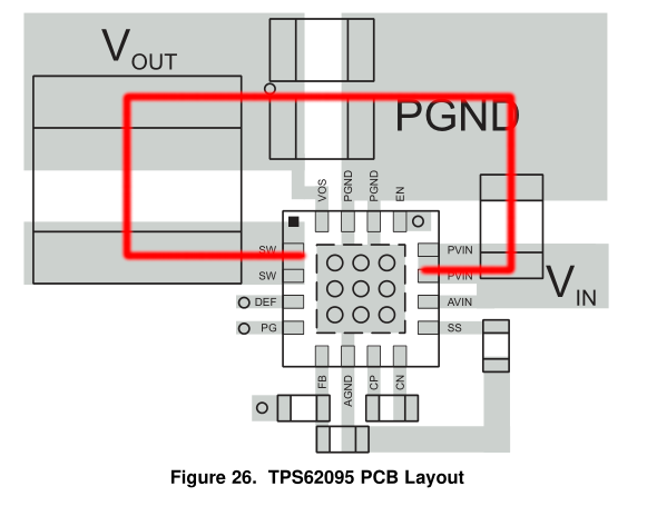
The output of the SW pin is going to be a high current 1.4Mhz switching signal. The current path flows through the inductor to Vout and Cout. This red line I have drawn above is called the power supply “hot loop.” Keep it as short as possible. This is just one of several layout considerations you should take; for a more comprehensive list, I would advise checking out AN-1149 from TI.
I’ve used an inner layer for power distribution. 5V is pulled around from its input power pin while most other power nets feed either the A33 or RAM. After staring at this screenshot for a while, I see many places for improvement, but this should do the trick. A general rule of thumb is 15mil/amp. However, the inner layers have less thermal dissipation, so we should double it.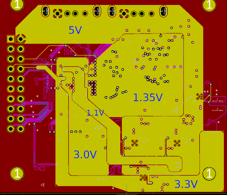
Bill of Materials Generation
In KiCad, working with components can be a pain. It would be best to end up with an automatic procedure to generate a CSV containing all the part numbers, manufacture, references and component quantity. You should then take that CSV and dump it directly into your part supplier’s BOM tool. One of KiCad’s shortcomings is its ability to group components by value (or other fields) and then apply one part number to the lot.
As an example: say I’ve placed 300x 1k, 1/4W, 0402 resistors in the schematic. I want to edit all of these parts to have a “Part Number” field with the manufacture part number. Unfortunately, KiCad can’t perform this grouping itself, so we’re shit out of luck; I had to edit every single field of the 1k resistors.
Just kidding, that would be the outcome if I were using bullshit closed source proprietary software. Since KiCad has an incredible community, xesscorp has built a tool called Kifield. This does exactly what I described, however, with one small issue I patched: https://github.com/xesscorp/KiField/pull/64. With purely numeric part numbers, the script would raise an exception. This was because Python uses type inference instead of explicit type specification (like in C). The function re.sub() expects a string, and since I used a purely numeric part number Python was inferring this as an int. This took me 10 minutes to figure out and is another great example of how proprietary software would have left me out in the rain.
The Build
After the design is finished, it’s time to order all the parts; I grabbed the parts from LCSC and boards from JLCPCB. I had to find someone on Alibaba to get the A33’s from, as this isn’t a standard stocked component.
I assembled the boards at Vancouver Hack Space, a communal space with everything needed for electronics assembly (and any other tools you require). To start, I taped the boards to the ground, then the solder stencil on top. Then I used a blade to disperse all the paste over the top layer of the boards.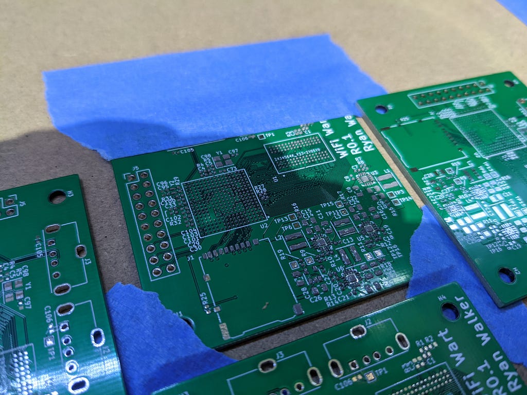
I then placed all the required top components with tweezers, and then it’s into the reflow oven!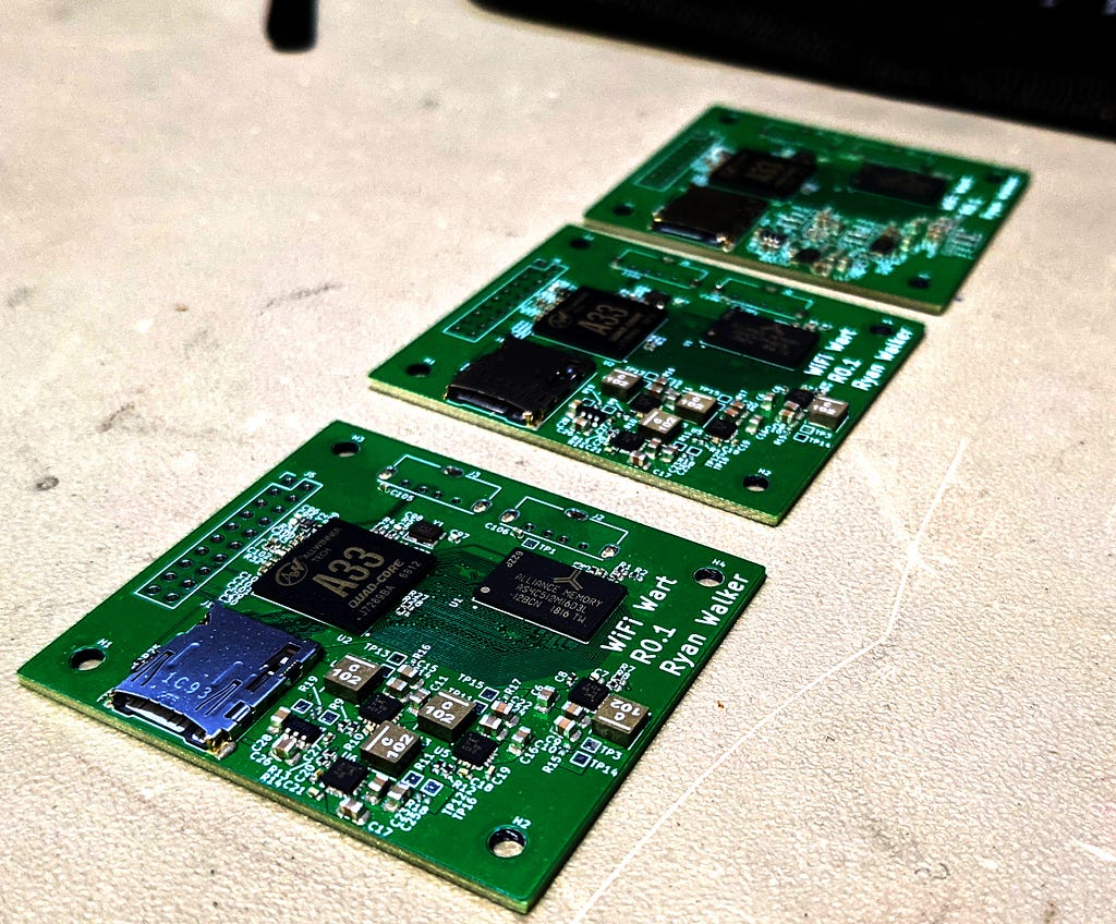
These boards require components on both sides because the A33 and RAM require decoupling on their internal pins; caps on the top layer aren’t close enough.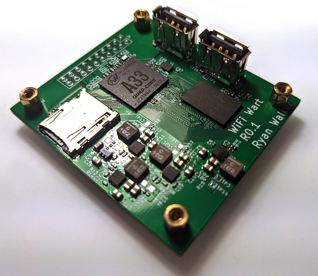
Bringup
A keen observer would have noticed the 0ohm resistors bridging the supplies’ output to their main power distribution rail. Isolating the supplies’ output from their load was done to verify the output voltage before connecting them to the rest of the electronics. An improper voltage could easily damage the downstream electronics. All the switching supplies worked as expected when firing up the boards, meaning the output voltage looked correct. If I were working for a client, I would check all the ripple on the rails under the continuous and discontinuous mode, load the rails with a digital load to check the thermals and supply current, check the transient response to ensure the supplies can react to dynamic loading, check the efficiency and check the quiescent current consumption. However, I’m not working for a client, so that a simple DMM check will suffice. I start by checking for dead shorts from the outputs to GND and outputs to other outputs. After this seemed okay, I fired on a current limited 5V@100mA supply and checked the outputs with a DMM on DC mode (ensure correct voltage) and AC mode (ensure the voltage isn’t switching all over the place). Everything seemed kosher.
There was one major design flaw with the power tree. The 2.5V linear regulator is derived from the 3.3V switching regulator, but the input of the 2.5V LDO is connected after the 0-ohm jumper. This means to test the 2.5V LDO, and I have to connect the 3.3V regulator to the rest of the system. Stupidly assuming that everything would be fine, I jumped all the rails into the system and fired it up. The 2.5V output was measuring 3.3V! I then frantically turned off the supply and sulked into my chair. This feeling only became worse after checking the datasheet for the A33 and realizing the absolute max rating of the DLL (2.5V) input was 2.75V. Electrical engineering is all about being meticulous and overly paranoid about everything all the time, which I failed to do. After the autopsy was complete, the problem was obvious. Somehow I ordered a 3.3V LDO instead of a 2.5V, even though the BOM lists the 2.5V part. Sad days, sad days for sure.
My goal for the end of this post was to get to a point where I was booting into the OS. However, things don’t always work out. I’ll have to order some new regulators and try with the other boards.
The Great Divide
Up until now, I have designed a single board that will be used for evaluation, and this is called the “non-form factor” board, or NFF for short. You have probably noticed that it isn’t the correct shape to fit inside the enclosure. This brings us to the great divide: the fork of the NFF board into the power form factor and compute form factor. The power board’s purpose is to take 250-120V and convert this to 5V using a flyback supply feeding the switching regulators. The regulators then convert 5V into 3.3V, 3.0V, 2.5V, 1.35V and 1.1V (just as on the NFF). The power board feeds all these rails into the compute board, containing everything else in the design, such as the A33 MPU, RAM, SD card slot, two WiFi radios and USB port. There are several pros and cons to going with a two-board system. I’ve designed several of these before, so let’s talk about it.
Pros of “two board system”
- You can rev each board individually. If you want to switch regulators on the power board and you have the inventory of the compute board, you don’t have to discard the compute boards.
- Noise isolation, you’re physically moving all the switching regulators away from the sensitive electronics.
- Different board manufacturing capabilities. I might choose 1oz copper for the compute and 2oz for the power. Compute might need 4 layers while the power only needs two layers.
- Vertical space gain. There is a lot of horizontal board space taken by the BGA, RAM, SD card and radios. However, there is very little vertical space required. By stacking two boards, I’ve doubled the horizontal space.
Cons
- Cost. It’s more expensive to build two boards instead of one.
- Signal Integrity. If you have high-speed signals running between boards, you have to worry about the SI of the board-to-board connector.
- Assembly time. Gotta plug em together, yo.
- Mechanical design and interface.
As for the design of the two boards, I’ve chosen the RTL8188CUS module because of its super small size (10mm x 11mm) and simplicity of wiring. So I’ve created the part and dropped those into the compute board. The form factor stuff will be a tight design, so I want all the CAD of the parts in the design, so I drew up the RTL in FreeCAD.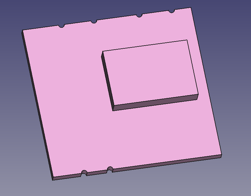
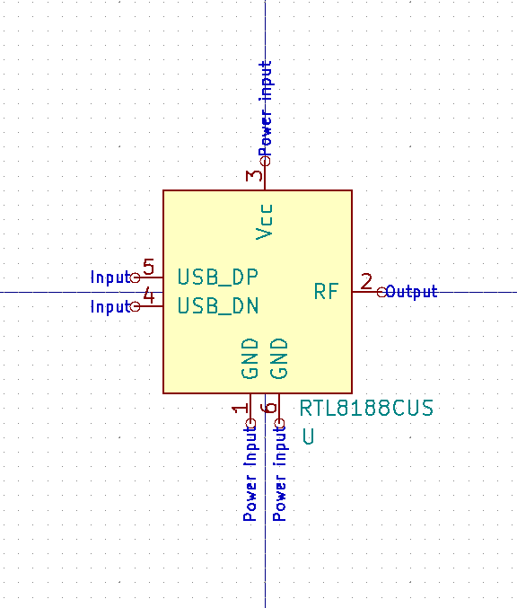
Here is the schematic symbol. It just works over USB and needs a simple 3.3V rail.
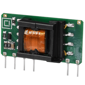
As for the mains to 5V flyback supply, I quite like CUI’s PBO-15C-5. This is a 15V flyback supply that contains the magnets, IC’s and support components to make the magic happen. I would consider it a “semi module” as you still need to supply larger caps and inductors external to the board. I like the vertical form factor. As for getting this through regulations, it’s going to be a lot easier than a discrete design.
One critical design note is: CY1 needs to be a Y1 safety capacitor. This is because, except for the transformer, it’s the one component that connects the mains to the low voltage (LV). So if this part fails, it will connect mains to the USB port, which is obviously extremely dangerous.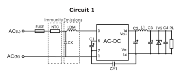
Another safety note is mains/LV isolation. You want to take a look at a creepage and clearance table. Creepage is the distance between high voltage and low voltage with the board in between, while clearance is the distance through air. Please note this isn’t an extensive safety overview, primarily because I haven’t done a safety audit yet or even been focusing on it. Always take extreme care when working with mains electronics!
The Mech
I am not a mechanical engineer. Until now, everything I’ve talked about has been in my wheelhouse. Now we’re getting into the sketchy stuff. The upshot is I have lots of mech friends, so I can bring them my crappy design to laugh at and eventually help fix.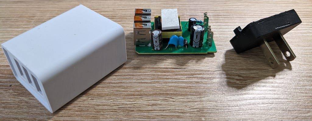
I took mechanical inspiration from the low-cost wall charger pictured above. I use the term “took inspiration” and not “copy” simply because copying this is synonymous with copying the dumbest kid in school. However, there are some parts I like: the over-moulded contacts and the slot where the PCB slides in are quite nice. So when the time comes to get a tool cut, it should be pretty straightforward? The two boards will stack vertically and connect with a normal 0.1" header (for now). There are some alignment features on the inside that will allow the boards to slide into the enclosure.
As per usual, I’m going to leave you with a render of what I have so far.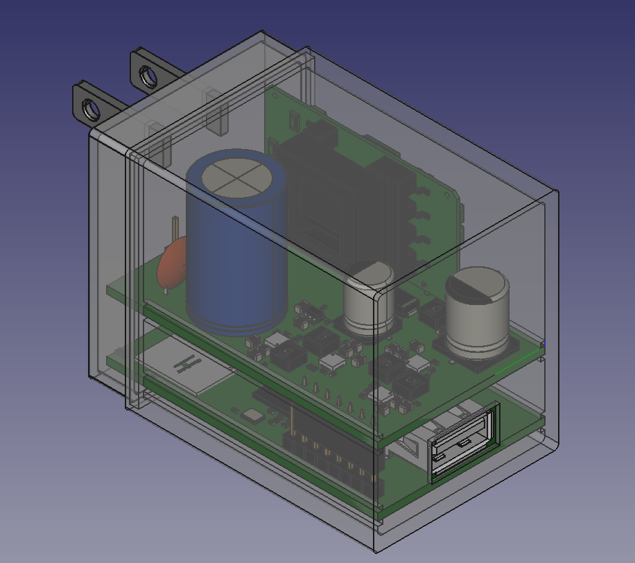
Until next time! :)