Up Until Now
The WifiWart is a powerful embedded Linux WiFi security device hiding inside a phone charger. It is akin to the WiFi Pineapple without looking malicious. Over the length of the project, I’ve had plenty of comments telling me to buy a single-board computer (SBC), jam in an existing enclosure, and call it done. If I was trying to build a one-off device for personal use, this is what I would do. But this project isn’t for me; it’s for the community. In the past six months, I’ve designed a completely open source SBC boasting a 1.2Ghz quad-core processor, 1GB of DDR3 RAM, two WiFi radios, a USB port and all the power supplies to convert mains electricity to the required voltages for the processor. In addition to the electronics, firmware and mechanical design open source, the CAD software used in the design is also open source. I did this intentionally, as having an open source design in Altium or Solidworks is pointless because nobody will shell out 10k+ for software to view my design. That being said, I hope you enjoy the final post :).
The Build
Before starting, I should say: working with mains electronics is inherently dangerous. If you choose to do so, this is solely at your own risk.
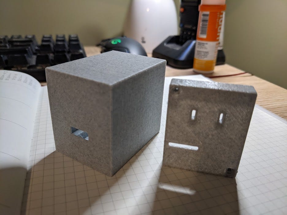
I started by 3D printing the enclosure. The print was done in PLA with my Monoprice Mini.
It was then time to assemble the two boards. Board assembly usually follows this process.
- Solder paste is applied using a solder stencil.
- Tweezers are used to place all the parts on the boards.
- Boards are heated using a reflow oven or hotplate.
- The solder paste reflows in a molten state, creating permanent solder joints.
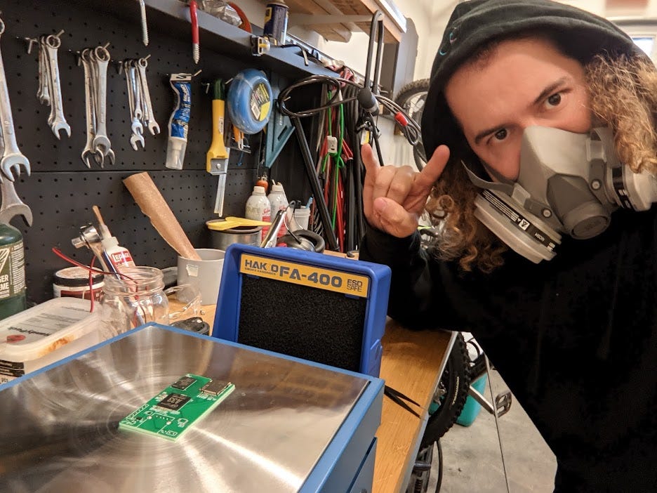
Compute Boards on the hotplate
Most of the board uses 0402 size passive components, which are 1mm x 0.5mm. These are some of the many components that are soldered on the board.
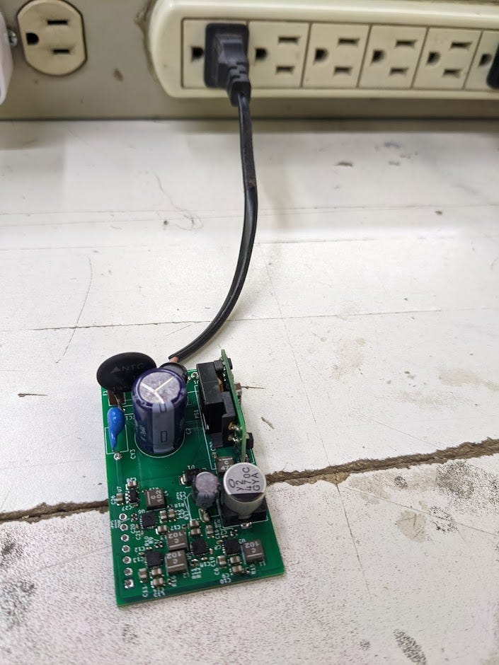
After the compute boards were finished, I built and tested the power boards.
Newer readers may not be aware, but the power board stacks above the compute board as pictured below. The power board is responsible for converting mains to 5V and creating all the other voltage rails required by the central processor. The compute board houses the microprocessor, RAM, WiFi radios etc. For lots of details on the electrical design, you might find Part 1 interesting.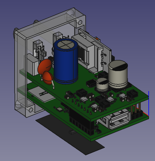
I then glued the contacts into the enclosure; these parts will be over-moulded during the injection moulding process in the final design. It’s essential these contacts are secure in the device; if they come off in an outlet, someone would get hurt. I wouldn’t trust my glue job for anything other than a prototype handles by myself alone.
The mains blade contacts interface to the PCB through friction fit contacts are shown below.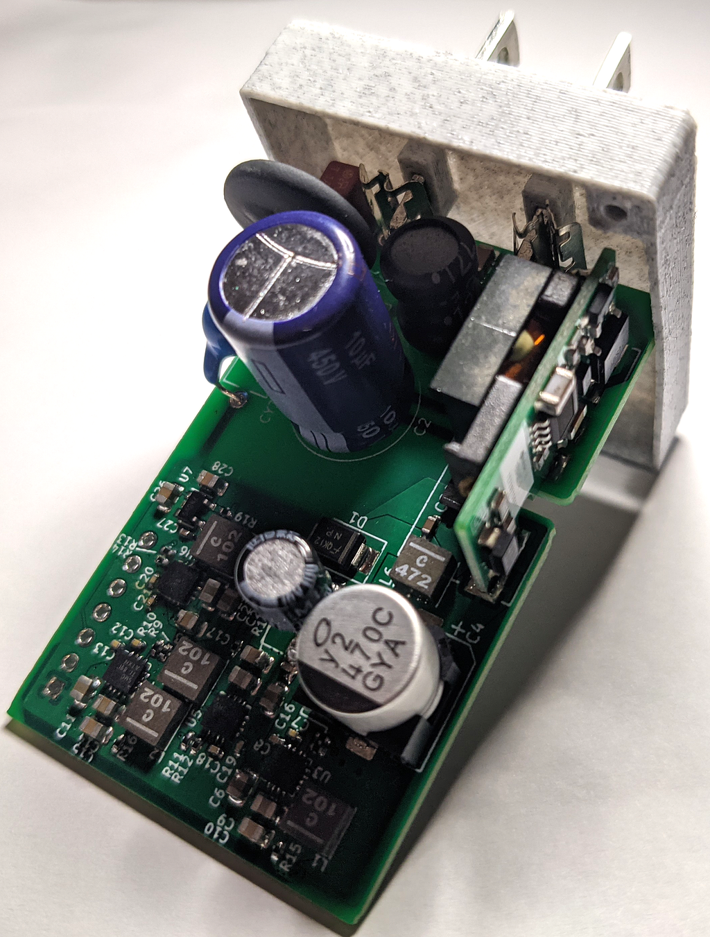
Final Assembly
After six months, I finally have the prototype completed. I flashed the OS to the SD card, fired it up, and the UART logs looked fine. If you want more details about what I just said, part two has lots of details on building and configuring the OS.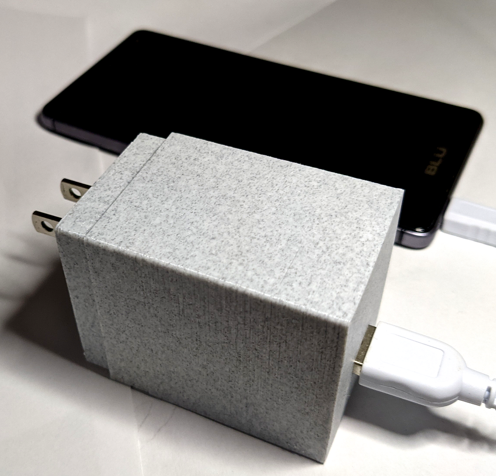
What’s next
I was planning on getting a crowdfunding campaign going, but the chip shortage ruined those plans for now (more on the chip shortage in part three). I don’t want to pivot over to other untested chips, so the crowdfunding will have to wait. I want to thank all the support I have received through the security and open source community.
I own and operate a small consulting company; if you or anyone else needs help with this type of engineering work, I would love to hear from you!
